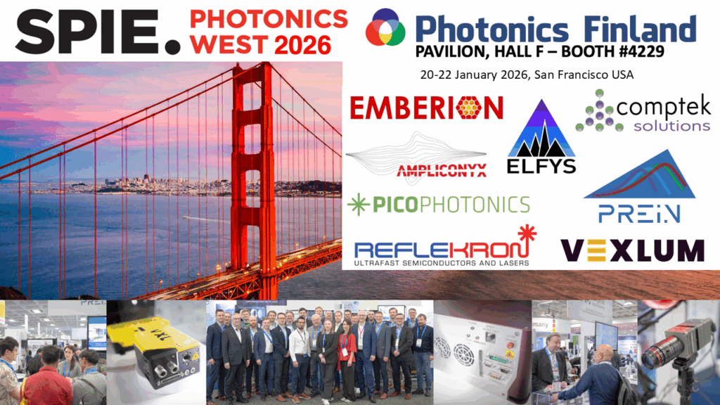
PREIN Flagship together with Photonics Finland and 7 Finnish photonics companies join Photonics West 2026 with a joint booth. PREIN related presentations are from 17 Jan to 22 Jan.
SPIE Photonics West is the premier event for lasers, biomedical optics, optoelectronics, and technologies supporting biophotonic, quantum, and vision applications.
PREIN booth #4229 at the Photonics West fair, see here
Photonics West 2024 floor plan, see here
Here you have a chance to meet researchers and company representatives in the field of photonics. SPIE Photonics West is the main event and exhibition for many Photonics Finland member companies! PREIN Flagship participates in Photonics Finland booth and the exhibition provides an excellent place to meet researchers and company representatives in the field of photonics.
PREIN Research in the SPIE Photonics West Conferences
With nearly 100 conferences and 5,000 presentations featuring the latest research, SPIE Photonics West covers four large thematic areas:
- BiOS, the largest biomedical optics and photonics conference
- LASE on laser technologies and applications
- OPTO showcasing developments in optoelectronic devices, components, and materials, and their integration for commercial applications
- SPIE Quantum West conferences and Business Summit
There will be 23 academic presentations by PREIN researchers from all the four PREIN partner organisations.
PREIN related presentations
Saturday 17 January 2026
Power scaling of high purity OAM beams for biomedical applications (Invited Paper)
17 January 2026 • 3:40 PM – 4:10 PM PST
Presenter: Regina V. Gumenyuk, Tampere University
Abstract
We demonstrate an approach for power scaling of complex light structure with exceptionally high modal purity by coherent beam combining. This simple and robust technique can be applicable for any type of laser systems, and scaled with number of channels. This approach can open a pathway to more efficient and compact medical isotope separation systems or downscaling of Laser Wakefield Accelerators.
Tuesday 20 January 2026
High-power/energy all-fiber nanoseconds pulsed MOPA system based on Yb-doped spun tapered double-clad fiber
20 January 2026 • 2:20 PM – 2:40 PM PST
Presenter Hossein V. Fathi Tampere University
Abstract
We demonstrate a high-energy, narrow-linewidth nanosecond MOPA system based on a spun tapered double-clad Yb-doped fiber (sT-DCF) without using any external SBS suppression techniques. The system delivers 1.6 mJ, 115 MHz linewidth, 8 ns pulses at 100 kHz with 188 kW peak and 160 W average power at 76.6% slope efficiency. High quality spatial, spectral, and polarization properties are preserved throughout amplification. The sT-DCF design effectively mitigates SBS while maintaining excellent beam quality (M² ≈ 1.3) and a degree of polarization >97.5%. This work enables compact, high-performance fiber laser sources for demanding applications like coherent LIDAR and spaceborne spectroscopy.
Integrated photonics on titania-polymer hybrid platforms
20 January 2026 • 3:20 PM – 3:40 PM PST
Presenter: Matthieu Roussey, University of Eastern Finland
Abstract
Titanium dioxide (TiO₂) is an attractive material for integrated optics due to its high refractive index and broad transparency. Using Atomic Layer Deposition (ALD), we fabricated two complementary photonic platforms with ultra-low-loss TiO₂ layers. The first is a strip-loaded waveguide on oxidized silicon, achieving propagation losses as low as 7 dB/m. The second is a vertical nanowaveguide (200 × 800 nm) formed by ALD filling, supporting a fundamental TM mode with bend radii down to 7 μm and >95% transmission. These platforms enable low-loss guiding and tight bends, paving the way for integrated circuits such as spirals, interferometers, and beam splitters.
Regrowth free monolithic integration platform on GaAs using vertical twin waveguides
20 January 2026 • 5:20 PM – 5:40 PM PST
Presenter: Kaveh Ebadi, Aalto University
Abstract
In this work we present a design for regrowth-free monolithic integration on GaAs for lasers and PICs in the 9xx nm wavelength range. The design consists of active and passive waveguides vertically separated by a low refractive index spacer layer. Light is transferred between the active and passive waveguides via adiabatic tapers enabling fabrication of separate active and passive components. Here we will present the coupler design and recent progress towards device fabrication.
Wednesday 21 January 2026
Controlling quantum entanglement with structured light (Keynote Presentation)
21 January 2026 • 8:30 AM – 9:10 AM PST
Presenter Robert Fickler, Tampere University
Abstract
Using the nonlinear process of quantum frequency conversion, we show that structured light can be leveraged to convert an entangled photon to another frequency, thereby also changing its quantum state from spin to orbital angular momentum. Moreover, by adjusting the classical non-separability between spin and orbital angular momentum of the structured light field, we are able to control the degree of entanglement of converted photon pair. As our scheme can also be interpreted as a form of entanglement swapping where the structured classical field simulates an entangled pair of photons, it might be also interesting for future quantum networks and quantum communication schemes.
Thick-SOI PICs with tunable lasers, broadband filters, and low-loss fiber coupling (Invited Paper)
21 January 2026 • 4:00 PM – 4:30 PM PST
Presenter: Timo Aalto, VTT Technical Research Ctr. of Finland Ltd.
Abstract
Photonic integrated circuits (PICs) with 3 µm thick silicon-on-insulator (SOI) waveguides offer a unique combination of ultra-low propagation losses (3 dB/m), broadband fiber-coupling with <2 dB loss for both polarizations, ultra-broadband (>500 nm) wavelength filtering/multiplexing, small phase errors and dense integration. Low-loss waveguide-fiber coupling is demonstrated with 3D polymer structures patterned with two-photon polymerization. Different methods are reviewed for coupling SOI waveguides to semiconductor optical amplifiers (SOA), including flip-chip bonding, 3D polymer structures and fiber coupling. Broadband tunable lasers are demonstrated for data centre networks, and the related application needs in the DYNAMOS project are explained. These lasers are based on the Vernier concept, where multiple resonators and interferometers are combined to achieve >110 nm tuning range. Finally, access to this PIC technology through the new PIXEurope pilot line is explained.
Thursday 22 January 2026
Faking entanglement with unnoticeable small measurement errors
22 January 2026 • 9:20 AM – 9:40 AM PST
Presenter: Jaime Moreno, Tampere University
Abstract
Entanglement is a key resource for secure quantum communications. Consequently, many protocols depend on reliable entanglement certification. In this work, we propose a protocol to surpass the non-separability bound of an entanglement witness with separable states. We achieve this “faking” of entanglement through introducing a slightly perturbed positive operator-value measure (POVM) with a fidelity to the ideal POVM higher than 99%. In the experiment, we simulate photon pairs by splitting a faint fs-laser and prepare the separable state employing transverse spatial encoding using macro-pixels. We achieved an average detection probability of around 97% for dimensions d = 11, 19, 31, 43 and 61, and very low average crosstalk of 1:700. Through artificially introducing a perturbation to the POVM of only 0.35%, we were able to violate the non-separability bound for all dimensions and showed that it is easier to fake entanglement in higher dimensions.
Complex modulation of light in polarization and space using laser-written multi-plane light conversion
22 January 2026 •10:10 AM – 10:30 AM PST
Presenter: Oussama Korichi, Tampere University
Abstract
We present a compact and efficient realization of Multi-Plane Light Conversion (MPLC) for full vectorial light modulation, enabling control over polarization, phase, and amplitude. Conventional MPLC implementations based on phase-only modulation suffer from losses and limited polarization control, while metasurface-based solutions require complex nanofabrication processes. Our approach employs laser-written birefringent waveplates in silica slides, each with fixed retardance and a spatially varying optical axis orientation. The structures are fabricated using direct laser writing of nanogratings in silica, achieving ~90% transmission and ~1–2 µm spatial resolution. We demonstrate high-dimensional quantum gates and a polarization-controlled single-photon CNOT gate using spatial and polarization degrees of freedom. This cleanroom-free platform shows strong potential for high-dimensional quantum processing, optical communication, and beam shaping, with future prospects for extending modulation into the frequency domain.